- 您现在的位置:买卖IC网 > Sheet目录2009 > MAX19713ETN+T (Maxim Integrated Products)IC ANLG FRNT END 56-TQFN
MAX19713
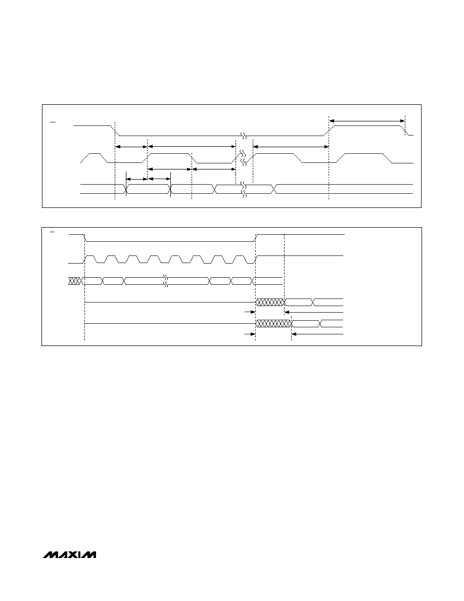
Figure 6. Serial-Interface Timing Diagram
tCSW
tCS
LSB
tCL
tCP
tCH
tDH
tDS
MSB
tCSS
SCLK
DIN
CS/WAKE
10-Bit, 45Msps, Full-Duplex
Analog Front-End
______________________________________________________________________________________
25
QSPI is a trademark of Motorola, Inc.
Figure 7. Mode-Recovery Timing Diagram
CS/WAKE
SCLK
DIN
16-BIT SERIAL DATA INPUT
AD0–AD9
ID/QD
DAC ANALOG OUTPUT
SETTLES TO 10 LSB ERROR
ADC DIGITAL OUTPUT SINAD
SETTLES TO WITHIN 1dB
tWAKE,SD,ST_ TO Rx MODE OR tENABLE,RX
tWAKE,SD,ST_ TO Tx MODE OR tENABLE,TX
MAX19713 enters the power mode determined by the
WAKEUP-SEL register, however, all other settings (Tx
DAC offset, Tx DAC common-mode voltage, aux-DAC
settings, aux-ADC state) are restored to their values
prior to shutdown.
The only SPI line that is monitored by the MAX19713
during shutdown is
CS/WAKE. Any information transmit-
ted to the MAX19713 concurrent with the
CS/WAKE
wake-up pulse is ignored.
SPI Timing
The serial digital interface is a standard 3-wire connection
(
CS/WAKE, SCLK, DIN) compatible with SPI/QSPI/
MICROWIRE/DSP interfaces. Set
CS/WAKE low to enable
the serial data loading at DIN or output at DOUT.
Following a
CS/WAKE high-to-low transition, data is shift-
ed synchronously, most significant bit first, on the rising
edge of the serial clock (SCLK). After 16 bits are loaded
into the serial input register, data is transferred to the latch
when
CS/WAKE transitions high. CS/WAKE must transi-
tion high for a minimum of 80ns before the next write
sequence. SCLK can idle either high or low between tran-
sitions. Figure 6 shows the detailed timing diagram of the
3-wire serial interface.
Mode-Recovery Timing
Figure 7 shows the mode-recovery timing diagram.
tWAKE is the wake-up time when exiting shutdown, idle,
or standby mode and entering Rx, Tx, or FD mode.
tENABLE is the recovery time when switching between
either Rx or Tx mode. tWAKE or tENABLE is the time for
the Rx ADC to settle within 1dB of specified SINAD per-
formance and Tx DAC settling to 10 LSB error. tWAKE
and tENABLE times are measured after the 16-bit serial
command is latched into the MAX19713 by a
CS/WAKE
transition high. In FAST mode, the recovery time is 0.1s
to switch between Tx or Rx modes.
发布紧急采购,3分钟左右您将得到回复。
相关PDF资料
MAX271ENG+
IC FILTER LOWPASS PROG 24-DIP
MAX274ACWI+T
IC FILTER ANALOG 8TH-ORD 28SOIC
MAX281AEWE+
IC FILTER 5TH-ORD BESSEL 16-SOIC
MAX294CSA+
IC FILTER LOWPASS 8TH 8-SOIC
MAX295ESA+
IC FILTER LOWPASS 8-SOIC
MAX3634ETM+T
IC CLOCK PHASE ALIGNER 48-TQFN
MAX3676EHJ+T
IC CLOCK RECOVERY 32-TQFP
MAX3872ETJ+T
IC DATA RECOVERY W/AMP 32-TQFN
相关代理商/技术参数
MAX19713ETN+TGH7
功能描述:ADC / DAC多通道 10-Bit 45Msps Full-Duplex Analog Front-End RoHS:否 制造商:Texas Instruments 转换速率: 分辨率:8 bit 接口类型:SPI 电压参考: 电源电压-最大:3.6 V 电源电压-最小:2 V 最大工作温度:+ 85 C 安装风格:SMD/SMT 封装 / 箱体:VQFN-40
MAX19713ETN-T
功能描述:ADC / DAC多通道 RoHS:否 制造商:Texas Instruments 转换速率: 分辨率:8 bit 接口类型:SPI 电压参考: 电源电压-最大:3.6 V 电源电压-最小:2 V 最大工作温度:+ 85 C 安装风格:SMD/SMT 封装 / 箱体:VQFN-40
MAX19713EVCMODU
功能描述:ADC / DAC多通道 RoHS:否 制造商:Texas Instruments 转换速率: 分辨率:8 bit 接口类型:SPI 电压参考: 电源电压-最大:3.6 V 电源电压-最小:2 V 最大工作温度:+ 85 C 安装风格:SMD/SMT 封装 / 箱体:VQFN-40
MAX19713EVCMODU+
功能描述:数据转换 IC 开发工具 MAX19710/13 Eval Kit RoHS:否 制造商:Texas Instruments 产品:Demonstration Kits 类型:ADC 工具用于评估:ADS130E08 接口类型:SPI 工作电源电压:- 6 V to + 6 V
MAX19713EVKIT
功能描述:数据转换 IC 开发工具 RoHS:否 制造商:Texas Instruments 产品:Demonstration Kits 类型:ADC 工具用于评估:ADS130E08 接口类型:SPI 工作电源电压:- 6 V to + 6 V
MAX19713EVKIT+
功能描述:数据转换 IC 开发工具 MAX19710/13 Eval Kit RoHS:否 制造商:Texas Instruments 产品:Demonstration Kits 类型:ADC 工具用于评估:ADS130E08 接口类型:SPI 工作电源电压:- 6 V to + 6 V
MAX1971EEE
功能描述:直流/直流开关调节器 RoHS:否 制造商:International Rectifier 最大输入电压:21 V 开关频率:1.5 MHz 输出电压:0.5 V to 0.86 V 输出电流:4 A 输出端数量: 最大工作温度: 安装风格:SMD/SMT 封装 / 箱体:PQFN 4 x 5
MAX1971EEE+
功能描述:直流/直流开关调节器 Dual 180 Out 1.4MHz 750mA Step-Down RoHS:否 制造商:International Rectifier 最大输入电压:21 V 开关频率:1.5 MHz 输出电压:0.5 V to 0.86 V 输出电流:4 A 输出端数量: 最大工作温度: 安装风格:SMD/SMT 封装 / 箱体:PQFN 4 x 5